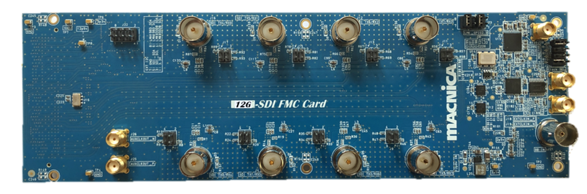
12G-SDI FMC Card R (Discontinued)
Expands to 8 channels of HD/3G/6G/12G multi-rate SDI interface
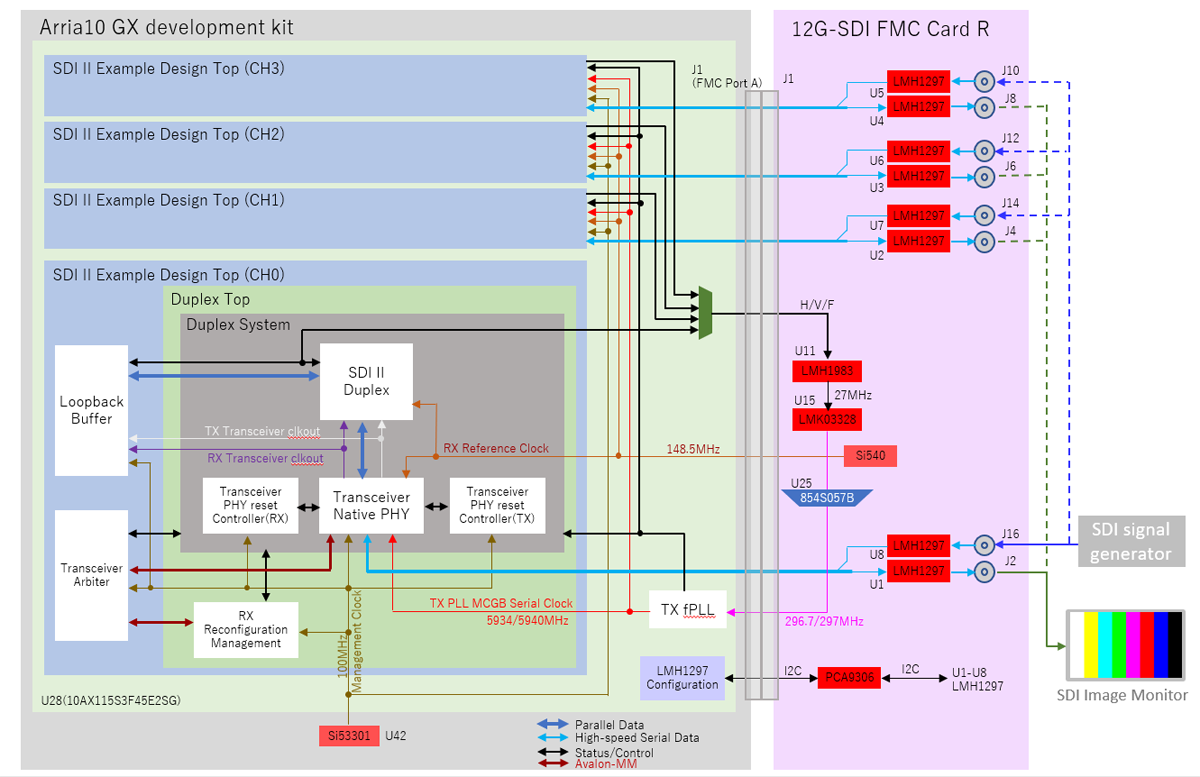
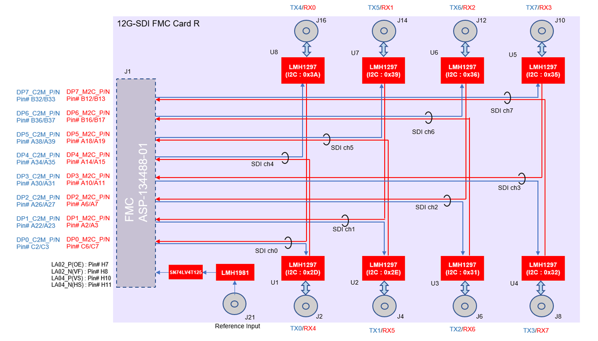
The 12G-SDI FMC card R is a daughter card that can be expanded to 8 channels of HD / 3G / 6G / 12G multi-rate SDI interface.
Each SDI channel can be configured as either an input or an output.
It has one BNC connector for external sync reference input and a pair of SMA connectors for external transceiver reference clock input.
The verified FPGA board of this card is the Intel® Arria® 10 GX FPGA Development Kit.
Features
|
Items |
Specifications and Part Numbers |
|---|---|
| Product Name / Part Number | 12G-SDI FMC CARD R / 12GSDIFMCCDR |
| Power Supply from FMC career | 3.3V, 1.8V(VADJ), 12V |
| Dimensions | 222.5mm x 69.0mm |
| SDI Interface | Input/Output x8 (Direction is configurable) |
| SMA Connector |
Differential clock input for FPGA transceiver reference clock x1 pair |
| BNC Connector | SDI input/output port x8 Samtec : BNC7T-J-P-GN-ST-TH1 Reference input x1 TE Connectivity : 5-1634503-1 |
| I2C Connector | I2C connector pins for external PC control |
| 12G-SDI Cable Driver/Equalizer | Texas Instruments : LMH1297RTV |
| Video Clock Generator | Texas Instruments : LMH1983SQE/NOPB |
| SD/HD Video Sync Separator | Texas Instruments : LMH1981MTX/NOPB |
| Ultra-Low Jitter Clock Generator | Texas Instruments : LMK03328RHS |
| Clock Multiplexer | IDT/Renesas : 854S057BGILF |
Packing List
| 12G-SDI FMC CARD R | 1 |
| M2.6 37mm Hexagonal Stainless Spacer | 4 |
| M2.6 10mm Hexagonal Stainless Spacer | 2 |
| M2.6 Pan Head Screw | 6 |
| Jumper Plug | 4 |
| Packing List / Precautions (Japanese) | 1 |
| Packing List / Precautions (English) | 1 |
SDI connection overview
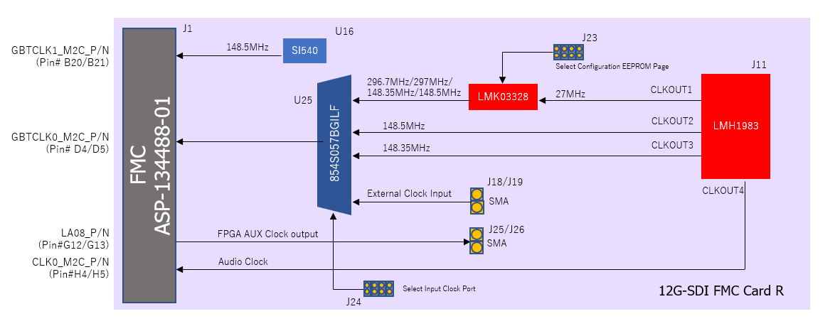
Clock Tree
Reference Design Block Diagram