
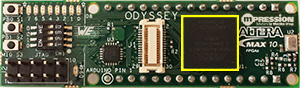
Odyssey MAX 10 FPGA Board Teardown
To make it easier to understand the engineering that's gone into the Odyssey MAX® 10 FPGA Evaluation board, we decided to tear down the board and go through the key components. We have also highlighted how some of the devices on the MAX 10 FPGA board that interact with devices on the Odyssey Bluetooth® SMART Sensor (BLE/Sensor) board that is part of the Odyssey MAX 10 FPGA Evaluation Kit.
For a schematic of the MAX 10 FPGA board design: [click here]
Full disclosure: We sell the devices shown here, so if you have a design that you expect to drive volume, please contact us so we can guide you to the best part for your application.
Main Processing Elements
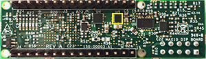
Altera 10M08 FPGA
An Altera® 10M08 FPGA is the featured device on the MAX® 10 FPGA Evaluation board. On this board, a single core voltage supply version of the MAX 10 FPGA is used in a space-efficient 169-pin UBGA that measures 11x11mm. Integrated features include analog-to-digital converters (ADCs) and dual configuration flash allowing you to store and dynamically switch between two images on a single chip. Unlike CPLDs, MAX 10 FPGAs also include full featured FPGA capabilities such as digital signal processing (DSP) blocks, PLLs, block memory, and soft DDR3 memory controllers (on certain devices). The MAX 10 FPGA also enables the use of the Nios® II soft core embedded processor.
For more information on MAX 10 FPGAs from Altera: [click here]
Switching and Input/Output Elements
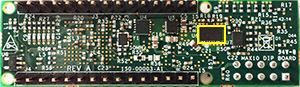
Analog Devices ADG788 IC Switch
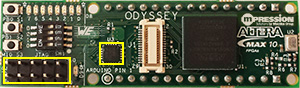
An Analog Devices ADG788 quad SPDT analog IC switch is used to switch the JTAG connection between the JTAG header (2x5 pin header from Wurth) and the connector from the BLE/Sensor board. When a USB Blaster is plugged into the MAX 10 FPGA board, it automatically switches the JTAG lines so that Max10 FPGA loading can be performed from a USB Blaster rather from the EFM32 Giant Gecko microcontroller on the BLE/Sensor board.
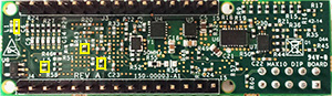
Wurth Electronik WE-SMCW LEDs
On the Odyssey MAX 10 FPGA board, mono-color bright green top view style LEDs from Wurth Elektronik is used for signaling.
Wurth Elektronik offers a broad family of LEDs in all colors (including white), various directional types and standard / ceramic packages. High reliability, low current requirement, fast switching, no UV/IR radiation, wide viewing angle and exceptional brightness even with small package sizes.
For information on Wurh Elektronik WE-SMCW LEDs: [click here]
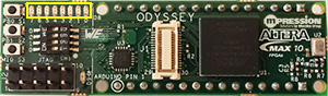
Switches, pushbuttons, and DIP pins
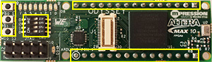
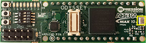
Other user IO is provided by DIP switches (Wurth), pushbutton switches (Omron), and two 15-pin gold plated headers (Wurth) that give the Odyssey MAX 10 FPGA evaluation board the appearance similar to the dual inline packages (DIPs) common in the ‘80s and ‘90s. This DIP structure is good for easy prototyping and debug. Additionally, a close look at the pinout shows that it's compatible with the Arduino Nano boards.
Note: Pin 1 on J4 does NOT align with the pin 1 silk screen label for Arduino on the MAX 10 FPGA board.
Audio input circuit
An interesting input option for Odyssey is the MEMS microphone from Invensense. Invensense makes versions of this tiny microphone with digital outputs, but this one drives an analog signal into a Linear Technology LT6220CS5 op amp used as a non-inverting gain stage (gain of about 72). This is then fed into one of the analog inputs on the MAX 10 FPGA.
Power Tree
The Odyssey MAX 10 FPGA board is designed to operate out on a desk, powered only by the USB on the BLE/Sensor board, or bread-boarded with power supplied from a bench supply (with or without the BLE/Sensor board attached). Also, the MAX10 FPGA has multiple IO banks that can run at different voltages. Odyssey is designed to allow two of these banks to be powered from a variable power supply through one of the DIP/header pins. If power isn't supplied to the variable rail, the variable banks default to 2.5V. A power diagram is shown below, and the components broken out separately after that.
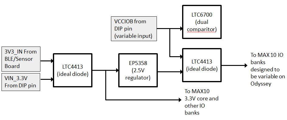
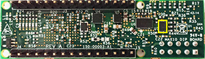
Linear Technology LTC4413 Dual Ideal Diode / Powerpath Controller
The Linear Technology LTC4413 dual ideal diode selects where to source the 3.3V board power from -- either the 3.3V_in DIP pin of the MAX 10 board or the power supplied from the BLE/Sensor board. The dual ideal diode does this seamlessly without the voltage drop associated with diode or'ing. This allows the MAX 10 board to be completely powered by the USB port on the BLE/Sensor board or from a bench supply when prototyping with a breadboard.
Enpirion EP5358 Power Regulator
The EP5358LUI PowerSoC is a tiny DC-DC switching regulator with built-in inductor that creates a steady 2.5V rail as an option for two of the MAX 10 IO banks. 2.5V is useful when driving LVDS or a 2.5V IO standard (2.5V LVCMOS for example). It provides up to 600mA of power at up to 93% efficiency. Requiring only an input and an output capacitor, the EP5358LUI achieves a tiny 14 mm2 footprint while being extremely easy to use.
For information on the whole family of space-conscious Enpirion PowerSoCs: [click here]
Linear Technology LTC4415 Dual Ideal Diode / Powerpath Controller
The Linear Technology LTC4415 dual ideal diode seamlessly selects the IO voltage for the variable I/O voltage rail on the MAX 10 FPGA without the voltage drop associated with diode or'ing. IO power can be supplied via a DIP pin or from the on-board 2.5V supply created by the Enpirion power regulator device.
Linear Technology LTC6700 Dual Comparator
A Linear Technology LTC6700-1 comparator is used in conjunction with the LTC4415 dual ideal diode to determine which MAX 10 FPGA IO rail supply to use. If the power supplied via the DIP pin falls into the range of 1.7-3.4V, the DIP pin power rail will be used to power the MAX 10 FPGA's variable IO banks. If the DIP supply falls outside of that range, the static 2.5V rail will be selected.
Linear Technology also has a number of other interesting options for the IoT market, such as their energy harvesting solutions: [click here]
Wurth Electronik WE-CBF Ferrite Beads
To help filter sensitive (analog) power rails on the board, the Odyssey design uses Wurth Elektronik WE-CBF ferrite beads. These SMD chip bead ferrites are placed directly on the PCB and offer excellent high-frequency filtering properties while maintaining a low DC resistance for minimum power dissipation. Wurth Elektronik offers high speed, wide band, and high current versions of the WE-CBF ferrite beads. In the Odyssey MAX 10 FPGA board design, wide band type WE-CBF beads are used with a maximum attenuation of 260Ω at 500MHz.
For information on Wurth Elektronik WE-CBF ferrite beads: [click here]