
3G-SDI FMC Card (Discontinued)
FMC daughter card for evaluation of 3G-SDI/HD-SDI/SD-SDI
 |
 |
|
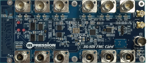
Top |
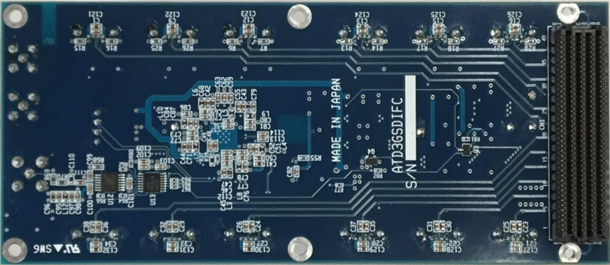
Bottom |
This card is an FPGA Mezzanine Connector (FMC) daughter card that complies with FMC ALTERA LPC+ standard. It is the card to expand functionality of FPGA evaluation board so that you can evaluate the 3G-SDI, HD-SDI, and SD-SDI interfaces by inserting this card into any one of various types of FPGA evaluation boards with FMC.
The evaluation board which has been verified to connect with this card is the Intel® Arria® 10 GX FPGA development kit.
Note: Intel® Arria® 10 GX FPGA Development Kit can be purchased separately.
Specifications
| External Dimensions | 69 mm x 160 mm |
| Printed circuit board | 6 layer FR4 |
| FMC | Samtec ASP-134488-01 |
| Power Supply | 3.3 V/VADJ (1.8 V)/12 V from FMC |
| Video sync separator | Texas Instruments LMH1981 |
| Video clock generator | Texas Instruments LMH1983 |
| Interface |
Active BNC TX x 6 |
Block Diagram
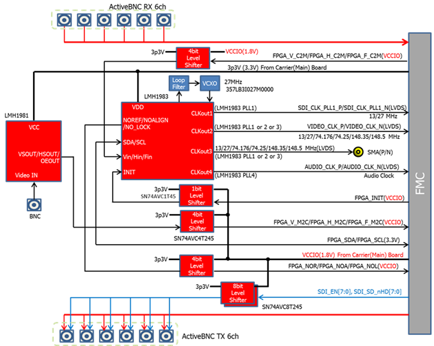
3G-SDI FMC Card Block Diagram
Evaluation Example
Using Intel® Quartus Prime 16.0 Transceiver Toolkit, you can test 2.97Gbps loopback between transceivers in Arria 10 GX.
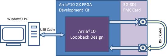
3G-SDI FMC Card Transceiver Toolkit Loopback Design Block Diagram
Ordering Information
| Product Name | 3G-SDI FMC CARD |
| Part Number | 3GSDIFMCCD |
Packing List
| 3G-SDI FMC Card | 1 pcs. |
|---|---|
| 37-mm spacer | 4 pcs. |
| 10-mm spacer | 2 pcs. |
| Pan-head screw | 6 pcs. |
| Packing list/precautions(Japanese) | 1 sht. |
| Packing list/precautions(English) | 1 sht. |