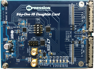
V-by-One HS HSMC Card (Discontinued)
HSMC daughter card for V-by-One HS IP core
V-by-One® HS is a leading-edge high-speed interface technology for flat panel display market developed by THine Electronics, Inc.
This daughter card can be used to verify V-by-One® HS Interface by connecting to HSMC connector of Intel® FPGA development board with V-by-One® HS Tx/Rx IP implemented.
In addition to V-by-One® HS Tx/Rx IP, you can also verify transceivers built in FPGA.
For your V-by-One® HS verification, in addition to preparing the Intel FPGA Development Board, you need to obtain a license (for evaluation or production) of Macnica V-by-One® HS Tx/Rx IP in advance.
The development board verified by Macnica for connection with this card is Intel® Cyclone IV GX FPGA Development Kit.
Features
| Interface |
HSMC, FX16 connecter by HIROSE ELECTRIC |
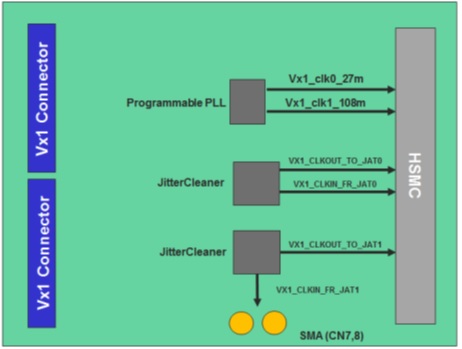
| Main devices | Si5317, IDT5V49EE504NLG, LT3029EDE |
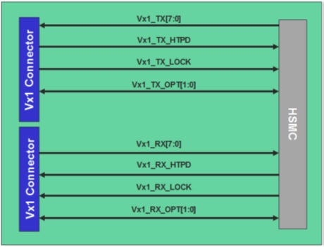
| Others | Can be connected to the evaluation board with HSMC Support 8 pairs of V-by-One HS interface Support V-by-One HS IP developed by Macnica |
Evaluation and Verification
Using the included FFC cable, you can evaluate both Tx and Rx at the same time by loopback connection with only one set of development kit and card, without preparing a separate kit for interconnection.
Block Diagram